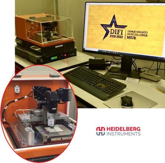
DIFILab hosts a nanofabrication research activity focused on the high-resolution lithography enabled by the novel NanoFrazor instrument.

The Nanofrazor is the first commercial instrument that allows direct surface nanostructucturing, even in three dimensions, via thermal-Scanning Probe Lithography. A nanoscale semiconductor tip is heated up in a controlled way to induce local nanopatterning of a thermo-sensitive material (Fig. 2a, b), also acting as a probe for in-situ imaging of the surface at the nanoscale.
This nanolithography has a strong potential in nanotechnology with impact in optoelectronics, nanophotonics, quantum technologies and biosensing.

Highlights
G. Zambito (Physics Department, University of Genova) has been selected as one of the winners of the Heidelberg Instruments Application Image Competition 2022/2023 on Advanced Nano- and Microfabrication (3rd prize, unique prize with a NanoFrazor application).
link to the video 'Fabricating Semiconductor MoS2 Nano-Circuits'

