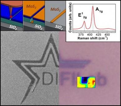
[1] Giordano, M.C., et al. "Deterministic Thermal Sculpting of Large‐Scale 2D Semiconductor Nanocircuits." Advanced Materials Interfaces 10, 5, 2201408 (2023). https://doi.org/10.1002/admi.202201408

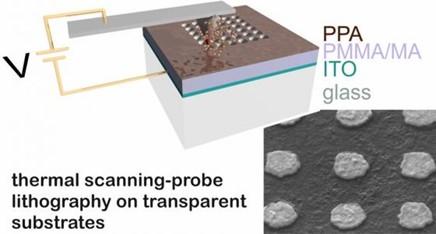
[2] Ramò, L., et al. “Thermal Scanning-Probe Lithography for Broad-Band On-Demand Plasmonic Nanostructures on Transparent Substrates” ACS Applied Nano Materials (2023). https://doi.org/10.1021/acsanm.3c04398

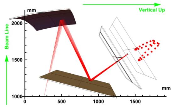
[3] Cardinale, R. & Petrolini, A. “Optical systems for future Ring Imaging Cherenkov detectors.” Nuclear Instruments and Methods in Physics Research Section A: Accelerators, Spectrometers, Detectors and Associated Equipment 1055, 168481 (2023). https://doi.org/10.1016/j.nima.2023.168481

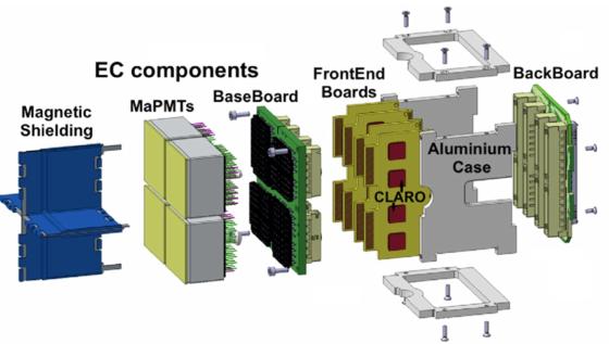
[4] Cardinale, R., et al. “Development of an integrated housing for Silicon Photomultipliers for future Ring Imaging Cherenkov photo-detectors.” Nuclear Instruments and Methods in Physics Research Section A: Accelerators, Spectrometers, Detectors and Associated Equipment 1055, 168476 (2023). https://doi.org/10.1016/j.nima.2023.168476


